3 Image Capture and Display
Digital radiography is very much like digital photography. The only difference between them is the means of depositing energy in the image receptor. In digital photography, visible light stimulates the detector. In digital radiography, invisible light (i.e. x-rays) activates the image receptor. So, the major difference between the two is a matter of photon energy and wavelength. Visible light has longer wavelengths and lower energy than x-rays. In fact, most cell phone cameras use a CMOS (complementary metal oxide semiconductor) sensor, which is one type of sensor used in radiology systems. The creation and display of images once they are captured is exactly the same. In this chapter we will break down the most common methods of image capture and examine the process involved in transforming the image signal into the display image.
Learning Objectives
Upon completing your study of this chapter, you should be able to:
- Describe the process of capturing image signal with a PSP plate.
- Explain the process of extracting the captured image data from the PSP plate.
- Summarize key features of the PSP system that distinguish it from other image capture systems.
- Identify the parts of a TFT array and their functions.
- Explain the process of capturing and processing the image signal with an indirect capture TFT system.
- Identify the materials used to create an indirect capture TFT image receptor.
- Explain the process of capturing and processing the image signal with a direct capture TFT system.
- Identify the materials used to create a direct capture TFT image receptor.
- Distinguish between direct and indirect capture systems based on the materials used in the image receptors.
- Distinguish between turbid and needle columnar scintillator structures.
- Explain the process of capturing and processing the image signal with a CCD/CMOS system.
- Identify distinguishing characteristics of the CCD/CMOS system.
- Explain the relationship between pixels, voxels and matrices.
Key Terms
Digital image receptor systems have replaced film-screen systems for recording radiographic images. While the technology underlying the capture of the image information varies by receptor system, the same basic process applies to all digital imaging systems:
- The remnant beam exits the patient and strikes the image receptor, depositing energy in proportion to the amount of radiation passing through the patient at that point.
- The imaging system converts (through a variety of ways) the x-ray energy into an electrical pulse.
- The electrical pulse is sent to an Analog-to-Digital Converter (ADC) where the pulse is measured and assigned a number (a process called quantization).
- The numbered data are sent to the computer in a string of numbers that are assigned positions in a grid according to the location they came from in the detector.
- The computer assigns each number a particular shade of gray based on the expected level of contrast for the part being examined.
- The number grid, with associated gray-tone assignment, is sent to a Digital-to-Analog Converter (DAC) which lines the data back up in a grid and displays it as an image.
Figure 3-1: Digital Image Capture to Display Process
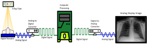
The basic process to get the radiographic image from image capture to display image involves converting the energy from the remnant x-ray beam to an analog signal, sending that signal through an ADC to change it into a digital signal, processing the image with the computer, sending the processed digital signal through the DAC which coverts it into an analog signal so it can be displayed on a video screen.
Now that we have a basic idea of how digital imaging works, let’s take a closer look at the types of digital image receptor systems.
Types of Digital Image Receptor Systems
There are basically 4 different types of digital image receptor systems – Photostimulable Phosphor (PSP), Indirect Capture Thin-Film Transistor (TFT), Direct Capture Thin-Film Transistor and Charge-Coupled Devices (CCD)/Complementary Metal Oxide Semiconductors (CMOS). In this section, we will examine how they capture image information.
Photostimulable Phosphor Systems
The photostimulable phosphor or PSP system was the first type of digital imaging system to be developed. It was first approved for clinical use in 1983. But in 1983, computers were the size of small office buildings and did not have hard drives for storing information. It took advancements in computer technology to drive the change to digital imaging in radiography. The PSP system is routinely referred to as “CR” in the radiography world. While CR officially stands for “Computed Radiography” all digital image receptor systems are both computed and digital. The primary distinguishing factor between CR and DR is the timing of the transfer of the image data to the computer for display. CR systems have a delay between capturing the image data and “reading” it to send it for display. CR systems always use photostimulable phosphor technology, because the crystals used in the phosphor plate have the ability to retain the image data for up to 48 hours.
There are 2 steps in using a PSP system: First, the PSP plate is placed under the patient and exposed to x-rays. Second, the plate is taken to a “reader” where the data is extracted from the PSP plate. Let’s take a closer look at the PSP plate.
The PSP Plate
The PSP plate consists of a layer of fluorescent phosphor crystals painted onto a durable plastic base and covered with a protective film. Remember from chapter 1, that fluorescence is the emission of light after stimulation with electromagnetic energy, like x-rays. Substances that fluoresce when stimulated with x-ray energy are called phosphors. There are several substances that fluoresce, but PSP plates are primarily made of Barium Fluorohalides with Europium activators. Halides include elements that have the same chemical properties like fluoride, bromide and iodide. These halides are pretty interchangeable in PSP construction and vary by manufacturer. The Europium is actually the magic ingredient. Europium has the ability to trap electrons in an excited state. This is what gives the PSP phosphors the ability to record the x-ray exposure for a limited amount of time.
Special Properties of Europium
Because of the way electrons fill the orbital shells, Europium has electrons in its P-shell even though its O-shell doesn’t contain the maximum number of electrons it can hold. These vacancies in the O-shell give the atom flexibility for the electrons in lower orbitals to move back and forth between their normal locations and these vacancies. The area of vacancies is called a conduction band. See Figure 3-2. To travel into the conduction band, electrons must absorb some energy to have the kinetic energy required to move further away from the nucleus. When electrons drop back down from the conduction band to their normal electron shell (also called the valence shell), they must lose that extra energy. The extra energy is released as an electromagnetic wave in the visible light spectrum. This is how some materials fluoresce.
But Europium is even more special. Within the conduction bands of Europium, there are some areas where electrons that jump up a level can get stuck. These areas are called electron traps or F-traps. This allows Europium delay some of its fluorescence until we can measure it.
Figure 3-2: Conduction Band in Europium Atoms
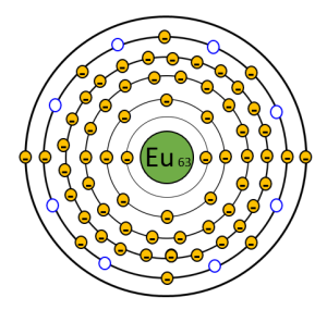
Europium atoms have vacancies in the outer few electron shells. The vacancies provide the opportunity for electrons to move between orbitals. This area is called the conduction band. The blue circles in the diagram represent F-traps, locations where electrons can get stuck.
PSP Plate Exposure
When x-rays strike the phosphor crystals in the plate, they transfer energy to the electrons in the Europium atoms. The atom is not ionized, but the electron becomes excited. Because the electron now has more kinetic energy, it jumps up an orbital level into the conduction band. See Figure 3-3. Some of the excited electrons drop back down to their normal orbital and lose the excess energy as light, but some of the excited electrons get caught in electron traps or F-traps within the conduction band. The number of electrons caught in the conduction band in a particular area of the image receptor is proportional to the amount of x-rays that struck the plate in that area. The electrons stuck in the F-traps make up the latent image. The word “latent” is defined as existing but not yet developed or manifest; hidden or concealed. So, the idea of a latent image is that all of the information needed to form the image is present, it just has not been processed in a way that makes the information visible.
Figure 3-3: Excitation and Trapping of the Electron
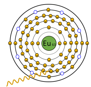
An x-ray that exits the patient interacts with an electron around the Europium atom. The x-ray transfers some of its energy to the electron, which give the electron the power it needs to jump up a level. The x-ray continues on with slightly lower energy. Sometimes the electrons drop back down to their valence shell immediately, but sometimes they get caught in the F-traps (seen in blue).
Extracting Image Data from the PSP Plate
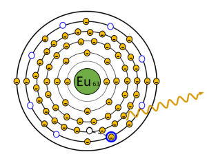
Once the latent image is captured in the PSP plate, the technologist takes the image receptor to the CR Reader. In the CR reader, the PSP plate is removed from its protective case, exposed to a laser light to release the trapped energy, erased and returned to the case. See Figure 3-4. The red helium-neon laser light in the CR reader scans the PSP plate back and forth in a zig-zag pattern known as a raster pattern. To avoid complex moving parts, the laser light is moved across the plate with a mirror or optical scanner that rotates to change the position of the laser. As the red laser light hits the phosphor atom, it gives a little extra energy to the electrons caught in the F-traps. This gives the electron enough energy to escape the trap. The escaped electron then releases the extra energy so it can return to its normal valence shell. The extra energy is released as blue-purple light. A light collecting system that is tuned to blue-purple frequencies follows the laser light and transmits the blue-purple light to a photomultiplier tube, where it is amplified and converted to electrical charge. Once we have an electrical charge, the process of creating the digital image is the same for all image receptor systems – The electrical charge is sent to the analog-to-digital converter to be measured and assigned a number according to the size of the pulse. Then, the numbers determined by the ADC are sent to the computer for processing into the displayed image.
The laser scanning process only releases about 50% of the electrons caught in the F-traps. To prevent ghost images from showing up on the next exposure, the PSP plate must be erased. To do this, the plate is exposed to very bright white light. This light knocks the remaining captured electrons out of their traps, leaving a clean plate for capturing the next image. The PSP plate is then returned to its protective cassette and ready for the next exam.
Figure 3-4: Reading the PSP Plate
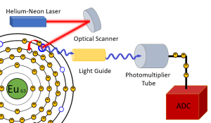
When the PSP plate is inserted into the reader, the plate is scanned with a Helium-Neon laser. The red laser light is directed across the plate in a zig-zag or raster pattern by the optical scanner. When the red laser light hits an electron caught in an F-trap, it transfers enough energy to the electron to allow it to escape the trap. As it jumps from the trap back to its normal shell, the electron releases blue-purple light. In the reader, a light guide follows the laser beam and transmits the blue-purple light to the photomultiplier tube. The photomultiplier tube absorbs the light and releases electron pulses. The electron pulses flow to the ADC to be measured and numbered and sent to the computer for processing.
Compared to other forms of digital image capture, there are several drawbacks to the PSP system.
- Only about 50% of the trapped electrons are released when the plate is scanned by the laser. While CR readers are designed to “erase” the PSP plate by flashing the plate with bright white light, occasionally this erasure does not happen, or the exposure is too high to be completely erased. This can cause ghosting – the appearance of one patient’s anatomy on the next patient’s image.
- Additionally, the spatial resolution of the image is dependent on the size of the laser beam and the frequency of “sampling” done by the light collecting system. While sampling the light more often can give us better detail, it causes the reading process to take much longer. Similar to film-based images, the technologist cannot evaluate the image while the patient is still in position due to the need for transporting the image receptor to the reader. This makes executing corrective actions more challenging as the patient has had several minutes to move around.
- PSP plates are sensitive to electronic noise from fluorescent lights and electricity running through the walls near where the plates are stored. Due to this sensitivity, the plates must be erased every 48 hours.
- Finally, there are a lot of moving parts in the CR readers. When parts physically move, they wear out and the machine breaks. This leads to more “down time” and interrupted patient schedules. The other forms of digital image capture move electrons and or light, but not the physical components within the systems. This make them more reliable than PSP systems.
Key Takeaways
- PSP phosphors are made of Barium Flurorhalides with Europium activators. Newer systems call the light emitting crystals “scintillators” instead of “phosphors”.
- Electrons becoming trapped in F-traps are an exclusive feature of PSP systems.
- Only about 50% of the trapped electrons are released by the laser light, so the plate must be erased with bright white light before reusing it.
- PSP plates are particularly sensitive to electronic noise and must be erased every 48 hours, if not used.
In 2016, the US government determined that CR systems did not provide the same quality of imaging as DR systems, and payments to hospitals and imaging centers using CR technology were progressively reduced through 2022, at which point exams performed with CR were not reimbursed through Medicare or Medicaid payment programs. This legislation has made CR systems obsolete in the US. (Interestingly, it was this same legislation that de-incentivized the use of film-screen imaging.) Digital portable machines were not widely available until this legislation was passed in 2016.
Activity 3-1: Image Capture and Display – The PSP Process
Test your knowledge of the order of events in capturing and displaying an image using a Photostimulable Phosphor plate.
Flat Panel Detectors
Flat-panel detectors were developed to address the shortcomings of the PSP systems. These detectors utilize an underlying structure called a Thin-Film Transistor arranged in a matrix or grid called an Active Matrix Array. Each cell of the active matrix array contains a sensing area, a capacitor for storing electrical charge, and a TFT transistor switch to release the stored charge. See Figure 3-5. Each cell in the active matrix array is known as a detector element or DEL. The percentage of the area within the DEL that is occupied by the sensing area is called the fill factor. TFT Arrays with higher fill factors capture more of the electrons from the x-ray interactions. Because of this increased capture efficiency, fewer x-rays can be used to reach an acceptable electronic signal. By using fewer x-rays we reduce patient dose. Because the size of the TFT and capacitor don’t vary much, smaller pixels have lower fill factors.
When a x-ray exposure is made, the x-rays cause the release of electrons in the sensing area of the DEL. This release of electrons can occur through a direct or indirect process (more on this below). The electrons migrate to the capacitor where they are stored. When we are ready to send the information to the computer, electrical impulses sent by the address driver down the gate lines to the TFT switches, open the gates and release the electrons from the capacitors one at a time. The released electrons flow down the data lines and through an amplifier before being sent to the analog-to-digital converter to be measured and assigned a number (a process called quantization). The numbers assigned to each DEL are sent to the computer for processing. The order the electrons are released in is controlled by the address driver and corresponds to the DEL’s location in the grid. That location will be used to position the information from that DEL in the display image matrix. In this way, the DEL is the functional unit of the TFT Array and the electrons it collects forms the basis for a single pixel in the image.
Figure 3-5: The Active Matrix Array
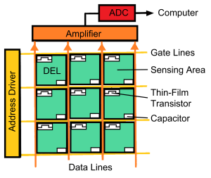
The active matrix array is composed of DELs arranged in rows and columns divided by gate lines and data lines. Each DEL has a sensing area, a capacitor and a TFT switch. During the x-ray exposure, electrons are released in the sensing area (by 2 different ways, see below) and the electrons migrate to the capacitors, where they are stored. When the x-ray exposure is complete, the address driver sends electrical signals down the gate lines to release the electrons from the capacitor. The TFT switch opens and the released electrons flow down the data lines to the amplifier, where the electrical signal is increased. From there the electrons flow to the ADC where the impulse is measured and assigned a number. The number is sent to the computer for processing of the displayed image.
Because all of the information captured by a single DEL is stored together in the same capacitor, the smallest resolvable area, and therefore the smallest structure we can see on the image is the size of the DEL. The DEL captures the information that will become the pixel in the display image.
Key Takeaways
- A DEL is composed of a sensing area, a storage capacitor, and a TFT.
- DELs that have a greater percentage of their total surface area dedicated to the sensing area have a higher fill factor and result in lower patient dose.
- Smaller DELs generally have lower fill factors because the sizes of the TFT and the capacitor don’t change.
- The capacitor stores the electrons collected in the sensing area.
- The address driver determines the order in which charges are released from the DELs.
- The process of measuring and numbering the electron pulses that is performed by the ADC is called quantization.
Activity 3-2: The Function of the TFT Array
Once the electrons reach the TFT Array, the process of converting them to a digital signal is the same. Test your knowledge of the order of events in converting electrons to a digital signal with a TFT array.
While the structure of the flat-panel detectors is the same, the configuration of the sensing area can vary. There are 2 basic types of flat-panel detectors – Indirect conversion TFTs and Direct conversion TFTs.
Indirect Conversion TFT Systems
In an indirect conversion detector, sometimes called a scintillator-based detector, the x-rays first strike a phosphor layer that is known as a scintillator. The term scintillation means sparkling or twinkling, which describes how the phosphor is releasing light. As we have seen previously, x-ray energy excites the electrons in the scintillator crystals. The electrons become excited and jump up into the conduction band. To return to their normal energy state, they release energy as light. The amount of light released is directly proportional to the amount of x-rays striking the crystal.
Figure 3-6: The Process of Indirect Conversion with TFT Detectors
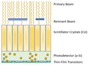
This image shows a cross-section of an indirect conversion TFT detector as it is exposed to x-rays. In the process of indirect conversion, the x-ray energy is converted to light by the scintillation crystals. The light from the scintillation crystals is converted to electrons by the photodetector. The electrons migrate through the photodetector layer to the capacitor where they are stored until released to go to the ADC.
As illustrated in Figure 3-6, the scintillator layer is applied to the top of a photodetector layer. The sensing area of an indirect TFT array is called a photodetector. The photodetector layer absorbs the light energy from the scintillator and releases electrons in proportion to the amount of light hitting the area. The photodetector is made of amorphous-silicon (a-Si), a special compound that is sensitive to visible light. (I remember that the photodetector in an indirect detector is made of amorphous silicon because indirect and silicon both have 2 “I”s.) The layer of the imaging plate that converts the light to electrons is called a photodetector because it detects the light that is emitted prior to releasing the electrons. The released electrons migrate through the photodetector layer are stored in the capacitor until the imaging plate is read. The stored electrons in the capacitors of each DEL form the latent image for TFT systems. When the address driver releases the electrons from the capacitor, they travel down the data lines, through the amplifier and to the ADC. The ADC assigns numeric values based on the number of electrons captured by the DEL, and then transmits the image data to the computer.
Activity 3-3: Image Capture and Display – The Indirect TFT Process
Test your knowledge of the order of events in capturing and displaying an image using an Indirect Capture TFT system.
Figure 3-7: Scintillator Crystal Formations
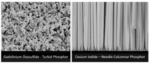
The clumpy looking turbid crystals of gadolinium oxysulfide allow light to spread out and dissipate as it travels to the photodetector. Gadolinium Oxysulfied crystals are seen above, left, in a scanning electron microscope image obtained by Alchetron, https://alchetron.com/Gadolinium-oxysulfide.
The needle columnar shaped crystals of cesium iodide direct light to the photodetector with little light spread or energy loss. Cesium Iodide crystals are seen above, right in a scanning electron microscope image obtained by Scinator, a company that produces and sells cesium iodide scintillators. https://scintacor.com/csi-%CE%BCm-scale-images-from-scanning-electron-microscope/
There are two basic options for scintillator materials – gadolinium oxysulfide or cesium iodide. Gadolinum oxysulfide (Gd2O2S) is a cheaper material, but is turbid in formation, which means the crystals are sort of random clumps. See Figure 3-7. When these turbid crystals release light, it goes in all directions (What is the technical term for that?). This means that some of the energy is lost out the sides and doesn’t reach the photodetector. It also means the light spreads out, so the light isn’t necessarily hitting the portion of the photodetector right below it, so the electrons may go into the wrong DEL, making the image more blurry. (The term turbid is actually defined as cloudy, obscure or blurry, which is appropriate since the images are blurrier when created with a turbid phosphor.)
While cesium iodide (CsI) is more expensive, the crystals of CsI have a needle or columnar shape. With crystals shaped like needles, the light travels down the crystal in a way similar to fiber optic cables and emerges at the bottom. This allows the light to be transmitted to the photodetector with very little loss of energy and very little light spread. This gives us higher resolution images. So, despite its higher cost, CsI detectors are the most commonly used indirect capture detector.
Key Takeaways
- A TFT system is considered “indirect” when it converts the x-ray signal to light before converting it to an electronic pulse.
- A scintillator converts the x-ray energy into light. The scintillator layer is most commonly made of either gadolinium oxysulfide or cesium iodide.
- Cesium iodide has a needle or columnar shape. This causes it to have less light spread than gadolinium oxysulfide and produce better spatial resolution.
- The sensing area of the TFT in an indirect system is called a photodetector.
- The photodetector captures the light from the scintillator and releases electrons. It is made of amorphous-Silicon.
Direct Conversion TFT Systems
In a direct conversion TFT detector system, the x-rays are converted directly into electrons. When creating the image with a direct conversion TFT detector, we do not need a scintillator. Instead, the TFT sensing area is going to capture the x-ray energy and convert it to light. We call this type of sensing area a photoconductor, and it is made out of amorphous-Selenium (a-Se). The amorphous-Selenium is capable of stopping the penetrating power of the x-rays. The x-rays interact with the atoms in the a-Se plate, ionizing the atoms and liberating electrons. The freed electrons migrate through the photoconductor layer to the capacitors. The capacitors store the electrons until it is time to send them through the amplifier to the ADC. See Figure 3-8. We call the active layer of direct conversion TFT detectors photoconductors because they conduct the electrons released by normal interactions with x-rays.
Figure 3-8: The Process of Direct Conversion with TFT Detectors
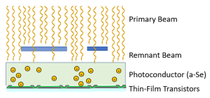
In Direct Conversion with a TFT detector, the x-rays interact with the amorphous-Selenium photoconductor, ionizing the atoms and liberating electrons. The electrons migrate through the a-Se sensing area to reach the capacitors. The electrons remain in the capacitors until they are released and sent to the ADC.
Activity 3-4: Image Capture and Display – The Direct TFT Process
Test your knowledge of the order of events in capturing and displaying an image using a Direct Capture TFT system.
Key Takeaways
- A TFT system is considered “direct” when it converts the x-ray signal directly into electronic signal without an intermediary step.
- The sensing area of the TFT in a direct system is called a photoconductor.
- The photoconductor captures the x-ray energy and releases electrons. It is made of amorphous-Selenium.
CCD/CMOS Systems
Charged Coupled Devices (CCD) and Complementary Metal Oxide Semiconductors (CMOS) are light sensors that are widely used in digital photography. Because of their sensitivity to light, we can use CCD/CMOS sensors to indirectly capture x-ray signals. Because the CCD/CMOS sensors need light, CCD/CMOS x-ray detector systems require the use of a scintillator. They use the same scintillators that are employed in the indirect TFT systems – Cesium Iodide or Gadolinium Oxysulfide. Again, Cesium Iodide is preferred due to its spatial resolution properties.
CCD/CMOS Sensor Structure
While in a TFT Array each DEL collects the signal for a single image pixel, a single CCD or CMOS chip can collect data for thousands of pixels. Inside a CCD or CMOS chip, the metal-oxide-semiconductor material forms a series of PN junctions like those found in the switches used to rectify the electricity flowing through the x-ray tube. Each PN junction only allows electrons to flow one way through it. The p-type section of the semiconductor acts like a capacitor. Each PN junction forms a diode, and each diode represents a pixel in the displayed image. As the silicon layer of the CCD/CMOS chip is ionized by the light photons striking it, the electrons released get stored in the p-type holes until the electricity applied to the CCD/CMOS sensor changes directions. As the electricity alternates directions, the electrons stored in each chemical capacitor shift to the next storage area in the line. This keeps the electron pulses separated as they are sent to the ADC. See Figure 3-9.
Figure 3-9: Internal Structure of CCD/CMOS Sensor
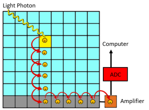
In this representation of the CCD/CMOS sensor, diodes are represented by each square cell. When light from the scintillator strikes an area of the CCD/CMOS sensor, electrons are released. As the electricity supplied to the sensor alternates, the electrons collected in each diode of the sensor move to the next diode in the column. The charges are moved sequentially through the amplifier and ADC before being sent to the computer for processing.
The challenge with CCD/CMOS systems is their much smaller size. The light emitted from the scintillator has to be compressed to fit on the smaller CCD/CMOS sensors. Accomplishing this reduction in the image size while maintaining the spatial integrity of the information requires the use of lenses and mirrors or other optical coupling devices. See Figure 3-10. Once the light from the scintillator strikes the CCD/CMOS sensor, the silicon layer of the sensor releases electrons. Other layers of the sensor store the electrons in a sequential pattern. At the end of the x-ray exposure, those electrons are then released line by line to be measured by the ADC.
Figure 3-10: The Process of Image Capture with CCD/ CMOS Detectors
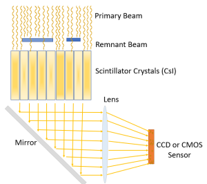
When using CCD or CMOS sensors, the x-rays strike the Cesium Iodide scintillator releasing light. The released light is directed from the scintillator to the CCD/CMOS sensor using either mirrors and lenses or other optical coupling systems (i.e. fiber optics). When the light strikes the silicon layer in the sensor, an electric charge is emitted. The electric charge is stored in a series of rows and columns that can be released sequentially when it is sent to the ADC.
Activity 3-4: Image Capture and Display – The CCD/CMOS Process
Test your knowledge of the order of events in capturing and displaying an image using a CCD/CMOS system.
The light optics employed in CCD/CMOS systems reduce the detail of the image. However, CCD/CMOS detectors have a faster refresh rate and require much less light to capture the image, making them an ideal system for digitally capturing fluoroscopic studies. Initially, CCD sensors produced images with higher quality and lower noise. But they were also larger, more expensive and used more energy than CMOS sensors. However, the large quality advantage CCDs enjoyed early on has narrowed over time and CMOS sensors are becoming the dominant technology.
Key Takeaways
- CCD/CMOS sensors require a scintillator to convert the x-ray signal to light. This makes CCD/CMOS systems a type of indirect capture system.
- CCD/CMOS systems require the use of mirrors and lenses or optical coupling devices to transmit and compress the light from the scintillator onto the CCD/CMOS sensor.
- Its higher sensitivity to low light levels and faster refresh rates make CCD/CMOS systems the best choice for capturing fluoroscopic images.
The Process of converting X-Ray Signal to Display Image
As we presented at the beginning of this chapter, there are common steps in converting an x-ray signal to a display image regardless of the image receptor system used (See Figure 3-10):
- X-rays energy is converted to an analog electronic signal – either directly or indirectly.
- The analog electronic signal is sent to the analog to digital converter (ADC) where each pulse is measured and assigned a number in a process called quantization.
- The numeric data are sent to the computer for processing (more on this next).
- Once processed, the data are sent through the digital to analog converter (DAC), which assigns a shade of gray to each number for each picture element (pixel).
- The gray scale information is sent to the video display monitor and address driver information is used to locate each pixel within the grid that forms the image.
Figure 3-10: Digital Image Capture to Display Process, Again
After capturing the x-ray signal contained in the remnant beam and converting that signal to electron pulses, we send the electron pulses to the ADC. The ADC measures the pulses and assigns each pulse a number. The sequence of numbers is the digital signal. The digital signal is sent to the computer for processing and the processed data is sent to the DAC. The DAC assigns a gray scale value to each number and sends those values to the video display monitor along with information that specifies where each piece of the image should be located.
Digital Image Properties
To understand how the computer processes the digital signal into an image, we need to have a basic understanding of the digital image. A digital image is made up of small boxes, or picture elements, called pixels that are arranged in rows and columns to form a matrix. See Figure 3-11. The pixels that make up the matrix are generally square. Each pixel is assigned a number that represents a brightness level. The number assigned to the pixel reflects the x-ray attenuation properties of the tissue that the pixel represents. The tissue volume represented by the pixel is known as a voxel (volume element).
Figure 3-11: Pixels, Voxels and Matrices
![]()
A digital image is created in a matrix – a grid of columns and rows of cells called pixels. Each pixel represents the volume of tissue the x-rays passed through before depositing energy in the detector element of the image receptor that corresponds to the pixel on the image.
The Role of the ADC
In the image capture and display process, the x-rays pass through the voxel – the patient’s tissue being imaged – and strike a particular location on the image receptor, depositing energy in the receptor. The location where the x-ray energy is deposited is determined by the DEL that stores the charge or its equivalent with PSP or CCD systems. The electrons stored in the DELs are released sequentially. The order that the electric pulses pass through the ADC forms the location information for the pulse. As each pulse passes through the ADC, the ADC measures it and assigns it a number based on its size. The size of the electron pulse, and the resulting number assigned to it are directly proportional to the amount of x-rays striking that area of the image receptor. The number assigned to the pulse becomes the numeric value of the pixel. Quantization is the process of assigning a numeric value to the electron pulses flowing from the DELs.
Figure 3-12: Quantization
The image above illustrates how the remnant beam exiting the patient combines all of the photons in a particular area into a single DEL. All of the photons striking the detector in the area of the DEL get combined and the numeric value is assigned to the pulse based on the total number of photons.
Matrix Size, Pixel Size and image resolution
The matrix size of the image is usually expressed in a multiplication problem x1 × y1. So the width of the image in pixels is the first number and the height of of the image in pixels is the second number. For example, the matrix in Figure 3-13, below, the matrix size of the image in the center is 9 × 8. To find the total number of pixels in an image, we just work the multiplication problem. Continuing with our example from Figure 3-13, 9 × 8 = 72, so the matrix in the center contains 72 pixels. The matrix on the right has a size of 20 × 19. When we do the multiplication, we find that the right image is made up of 380 pixels.
A larger matrix, when applied to the same space will result in smaller pixels. Smaller pixels will result in greater spatial resolution. Let’s take a look at these concepts in action. See Figure 3-13. The pixels are essentially trying to build a representation of the visual information with boxes. A pixel can only display a single shade of gray, so everything that lands within the pixel’s cell gets averaged together to determine the shade of gray that it will be assigned. If, as seen in image B, we divide the chest information into 2 inch pixels, areas of transmission and absorption get averaged together and the resulting image doesn’t really look much like the part. If we increase the matrix size to 20 x 19, as seen in Image C, the pixels are reduced to 1 inch squares to maintain the same field of view. Even though the image is still jagged or pixelated, we can see the basic shapes of the thoracic tissues begin to emerge.
Figure 3-13: Changing Matrix and Pixel Sizes
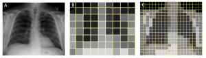
When creating a digital image, the image data from the patient’s tissues, as seen in Image A, are separated into a matrix of pixels. Smaller matrix sizes, like Image B are divided into fewer total pixels, so the pixels must be larger in order to contain all of the patient’s anatomy. In Image C, the matrix size is increased, which decreases the pixel size and results in an image that more closely resembles the anatomy it is intended to represent.
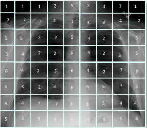
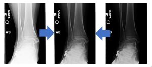
But we aren’t practicing radiography in the Minecraft world, and our images don’t look like stacks of blocks. Let’s look at this concept with real medical images. See Figure 3-14. The original radiograph of the femur, labeled A, has a matrix size of 1380 × 2021. If we reprocess the same image and save it with a matrix size of 171 × 250 (image B), and again with a matrix size of 68 x 100 (image C), we can see that the sharpness, or spatial resolution, decreases as the matrix size decreases. Spatial resolution issues are easier to recognize in structures with straight line, like the side marker and orthopedic hardware seen in these images. On image A, we can see fine details like the threads on the screws in the orthopedic hardware. On image B, we have lost the ability to see the individual threads and the right marker is looking a little fuzzy around the edges. On image C, we have almost lost the ability to tell the difference between individual screws and the side marker is pretty much unreadable. When we decrease the matrix size, but leave the field of view the same, the pixels have to get bigger in order to cover the same area.
Figure 3-14: Changing Matrix and Pixel Size on Medical Images
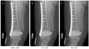
As the matrix size is reduced in this series of images from left to right, we see a decrease in resolution and greater pixelation.
Key Takeaways
Computer Processing of the Digital Data
Now that the electron pulses have passed through the ADC and we have converted the series of pulses into a series of numbers, we are ready to process those numbers with the computer. The events involved in processing the data into a display image include the creation of a histogram, comparing the histogram to an ideal histogram of the part, and rescaling the acquired data to most closely resemble the ideal image.
Histogram Creation
We know that the ADC analyzes the pulse of electrons coming from each DEL and assigns a number to the pulse. The size of the pulse is directly proportional to the amount of radiation the DEL absorbed during the exposure. We also know that the ADC processes the pulses in a particular order so we know the location each number is assigned to – the basis of the pixel in our image. A histogram is a bar graph. Mathematically, a histogram can be any bar graph, but in radiology, the histogram compares the exposure level to the number of pixels having that level.
To create the histogram, the computer counts each pixel that has the same assigned number and makes a graph of the total number of pixels vs. the number value assigned to the pixel from minimum to maximum values. In a way, creating the histogram is like cutting the image into pixels and stacking each pixel with the same value in a column. The resulting graph shows us the number of pixels per exposure level. If we organize each column so the exposure levels are in order from lowest exposure to highest exposure, we get an organized diagram of the overall exposure to the image receptor. See Figure 3-15.
Figure 3-15: Radiographic Histogram
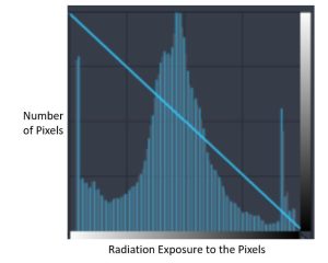
In radiology, a histogram is a bar graph that show the number of pixels having certain levels of radiation exposure.
Parts of the Histogram
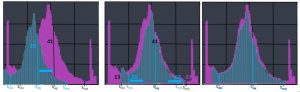
On radiographic images, the lower exposures are located on the left side of the graph and the higher exposures are on the right. This means that radiopaque tissues are represented by bars on the left side of the graph, while more radiolucent tissues are represented on the right. Histograms of radiographic exposures have a predictable shape. All images will show a large lobe that represents all of the tissues within the patient’s body. If the image receptor captured space around the patient’s body where the primary beam reached the IR, there will be a second, smaller lobe to the right of the one that represents the patient’s body part. This lobe represents the raw radiation captured by the image receptor. This is the most common histogram shape. Finally, if the patient has high attenuating matter within their body – orthopedic hardware or barium contrast media – there will be a third lobe to the left of the lobe representing the patient’s body part. We refer to this lobe as the metal lobe. See Figure 3-16. Note that some PACS systems may display the histogram data in the opposite order. Just watch for the indicator stripe at the bottom of the histogram that indicates whether the bar above it is bright or dark.
Figure 3-16: Types of Histogram Shapes
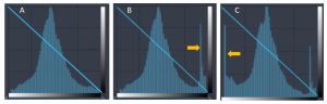
Image A shows a histogram of a standard pelvis. Since the anatomy extends off the image receptor, we only see the main lobe of the histogram that represents the anatomy. Image B shows a histogram of the pelvis on a smaller patient, where there is space between the patient’s anatomy and the edge of the image receptor. The lobe indicated with the yellow arrow represents the raw radiation. Image C shows a histogram of a knee on a patient with a knee replacement. In this histogram, we see the raw radiation spike on the right, but we also see the spike on the left that represents the metal in the image.
Identifying Values of Interest (i.e. Histogram Analysis)
Creation of a histogram from the raw data sent by the ADC is the first step in processing the data into a display image. Next, the computer must determine which portions of the histogram represent the patient’s tissue and which bars on the graph are outside the patient’s body or do not correlate to anatomical tissue. We call the pixels which represent anatomical structures values (or voxels) of Interest (VOI). In order to determine which areas of the histogram are important, the computer scans the histogram for landmarks. The computer scans the data inward from the right and left sides of the histogram. If there is no metal lobe, the first non-zero bar from the left is designated as Smin. Smin designates the lowest exposure value of interest. To find Smax, we must eliminate the raw radiation portion of the signal. To do this, the lowest bar graph from the right after the lobe created by the raw radiation is designated as Smax. See Figure 3-17. If the histogram has a metal lobe, a similar process is used to identify Smin.
Figure 3-17: Identifying Smin and Smax
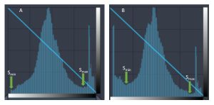
In image A, Smin is identified as the first non-zero bar from the left. In image B, because a metal lobe is present, Smin is identified as the lowest bar from the left after the metal lobe. Similarly, in both images, Smax is identified as the lowest bar from the right after the raw radiation lobe.
All of the values between Smin and Smax make up our VOI – voxels of interest or values of interest. The exposure to all of the voxels of interest is averaged to determine the Savg and the Exposure Indicator or Exposure Index (EI). The exposure index is a number estimating the overall radiation exposure to the image receptor for this body part. When this number is compared to average exposure for an ideal image of the same part, the EI gives feedback to the technologist for monitoring correct equipment use and observing variations in detector dose. While not directly associated with patient dose, the EI number can be used as a rough estimate of the overall dose to the patient.
Rescaling
Once we have identified the Smin, Smax and Savg, we know our VOI and can begin the rescaling process. Rescaling is the mathematical shifting of pixel values in the raw data to match the Smin, Smax and Savg of the reference histogram from the Look-Up Table. This shifting of the pixel values corrects the appearance of the image to display a consistent image brightness and contrast. A Look-Up Table (LUT) stores the ideal Smin, Smax and Savg for each type of image protocol. These default values are used to determine the initial display brightness and contrast.
The rescaling process takes place in 2 steps. First the Savg from the newly acquired histogram is compared to the Savg on the reference histogram from the Look-Up Table. To make the Savg equal in both histograms, the computer will add or subtract the same values to every pixel in the newly acquired histogram. In the example shown in Figure 3-18, the Savg for the blue histogram starts out lower (a value of 28) than the Savg for the pink reference histogram (a value of 41). This means that the computer will need to add the difference between the Savg for the reference histogram and the newly acquired histogram (41-28 = 13) to ALL of the pixels in the newly acquired data set. Adding 13 to all the pixels makes the Savg for the blue histogram equal to 41. This shift makes the newly acquired image have the same brightness as the image from the reference histogram.
Next, the Smin and Smax from the newly acquired histogram is compared to the Smin and Smax on the reference histogram from the Look-Up Table. In our example in Figure 3-18, the newly acquired data isn’t as wide as the VOI for the reference histogram. For the newly acquired histogram, the difference between Smin and Smax is 42 (63-21=42). For the reference histogram, the difference between Smin and Smax is 56 (69-13=56). This means that there were fewer different values collected in the new exposure that there were in the reference exposure. To make the Smin and Smax of the two histograms match, the computer will multiply the values of every pixel by the value that makes the columns of the blue histogram cover the same distance as the columns on the reference histogram. To calculate this for our example – 42 × X = 56, solving for X gives us 1.33. So to make the Smin and Smax match, the pixel values for the newly acquired histogram will need to be multiplied by 1.33. Because the VOI on the blue histogram is narrower than the VOI on the pink reference histogram, the blue pixels will need to be multiplied by a value greater than 1. If we needed to make our newly acquired data more narrow, we would multiply the pixels by a value less than 1. This shift makes the contrast of the image resulting from the newly acquired data roughly equivalent to the image produced by the pink reference histogram. Note that the rescaling process does not make the histograms match exactly. There are still variations in the histogram based on the patient’s tissues.
Figure 3-18: Rescaling the Raw Data
To make the image produced by the data associated with the blue histogram look as much like our reference image (pink histogram) we must perform rescaling. First, the Savg for the blue histogram is moved until it matches the pink one. This makes the average brightness of the images the same. Then blue histogram is stretched out (or squeezed together) to make the Smin and Smax align with the pink histogram. This makes the image contrast the same. Just because Smin, Smax and Savg now match, doesn’t mean the histograms are exactly the same.
Rescaling and the Resulting Image
So what does all this bar graph and math stuff have to do with my image? I’m glad you asked!
If we left the pixel values just like they were when they came out of the ADC, the display images would vary in brightness and contrast for every exposure that was taken (that is actually how life was when we were using film!). If the technical factors you set are a little too low, the image turns out too bright. If the technical factors you set are a little too high, the image turns out too dark. But rescaling can make even images created with 1/2x or 2x the optimum exposure look good! See Figure 3-19. Such extremes in technical factors can result in an acceptable looking images because digital imaging systems have a linear response rate.
Figure 3-19: Rescaled Images
Because the digital image receptors have a linear response rate, we can shift the values up or down into the optimum viewing range without losing image quality.
Linear Response Rate, Dynamic Range and Exposure Latitude
Figure 3-20: Quantum Mottle
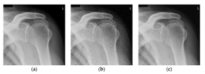
Quantum mottle is the grainy or speckled appearance of the image when too few photons reach the image receptor. Image A does not show quantum mottle. Image B shows significant quantum mottle. Image C shows a little quantum mottle, but the radiologists may find this level of noise acceptable in order to reduce patient dose.
These images were created by Nichole Morrissey on X-Rated https://radiography7.home.blog/2019/12/08/clo-16-describe-the-conditions-that-cause-quantum-mottle-in-a-digital-image/
Key Takeaways
- Rescaling involves mathematically shifting pixel values in the histogram of the acquired image so that the Smin, Smax and Savg match those in the reference histogram from the Look-Up Table.
- Rescaling is possible because the digital image receptors have a linear response rate.
- The linear response rate also gives us greater exposure latitude, the range of technical factors that will produce an acceptable image.
- Digital receptors have less latitude on the lower side than on the higher side of optimum technique because of quantum mottle.
- Quantum mottle is a graininess or speckled appearance of the image due to inadequate photons (or quanta) reaching the image receptor.
- Increasing technical factors beyond optimum to avoid quantum mottle leads to dose creep.
- Feedback with exposure index numbers and color coding helps reduce dose creep.
- The dynamic range of the receptor defines the upper limit of the number of shades of gray or number of variations in receptor intensity the system can identify.
Bit Depth
Bit depth refers to the number of shades of gray stored in an image. The higher the bit depth of an image, the more shades of gray it can store. The simplest image, a 1 bit image, can only show two colors, black and white. That is because the 1 bit can only store one of two values, 0 (white) and 1 (black). An 8 bit image can store 256 possible shades of gray, while a 24 bit image can display over 16 million shades of gray. In this way, the bit depth controls the numbers assigned by the ADC during quantization. As the bit depth increases, the file size of the image also increases because more gray level information has to be stored for each pixel in the image.
When thinking about the range of x-ray signals, they are monochrome, meaning that the digital signal comes in the form of a grey level, ranging from pure black to pure white. The more intense the analog signal, the whiter the grey level, meaning that radiographic images are typically displayed as a grey-white signal on a dark black background. The signal is spread across the available range of grey levels, the greater the amount of signal, the more grey levels needed to fully display the image. If a signal had a range of 5000 different exposure levels, but the system could only display 100 different grey levels, the signal would be compressed and every 50 exposure levels would be converted to one gray level, meaning that a signal would have to increase by over 50 exposure levels before a change could be seen in the image. This would make the system insensitive to small changes in attenuation. This is the primary reason we limit our image gray scale assignments to only the values of interest. By omitting the high and low exposures that aren’t related to the anatomical structures, we reserve the available gray levels for demonstrating tissues that matter.
In order to produce the correct number of grey levels to display the range of differential absorption, imaging systems can operate at different bit depths. Computers store information as ‘bits’, where a bit can be 1 or 0. If a pixel was 1 bit, it would either be pure black or pure white and would not be useful for radiographic imaging. Each bit can display 2x grey levels, so 1 bit is 2 (21) grey levels and 2 bits is 4 (22) grey levels. Medical images produced by x-ray detectors typically contain between 12–16 bits/pixel, which corresponds to 4,096–65,536 shades of gray. To benefit from the level of detail captured in these images, the images must be visualized by means of medical displays that have an equivalent number of available number of gray shades. For a long time medical LCDs only supported 8 bits or 256 shades of gray per pixel. Currently medical displays are optimized for mammography, increasing the available number of gray levels to 1,024 (10 bit). Figure 3-21 illustrates the visual differences changes in bit depth can make.
Figure 3-21: Bit Depth in Abdominal Imaging
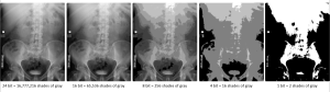
While the images displayed with 1, 4 and 8 bit depth show obvious loss of detail, it is much more difficult to distinguish the difference between the 16 and 24 bit depth images. (or perhaps my monitors are not configured to display greater than 10-bit images….)
Matrix size, Bit Depth and File Size
We know that larger matrices give us higher resolution and therefore better diagnostic quality. We have also seen that increased bit depth gives us greater perception of tissue differences. But both of these choices impact image file size and the overall storage capacity needed for a radiology department to function. To calculate file size we use the formula:
When we are dealing with file sizes in the megabyte (MB) and gigabyte (GB) ranges, it also becomes important to be able to convert between bytes and larger unit designations.
The process of combining values from adjacent pixels in an image to improve signal-to-noise ratio (SNR). Binning results in reduced spatial resolution.
The detector element; The smallest resolvable area in a digital imaging device.
A look-up table (LUT) is a series of mathematical equations that are used for post-processing in radiography. The LUT contains reference values for the maximum, minimum and average brightness expected for the exam type selected. The computer uses algorithms to mathematically adjust raw data values to control the brightness and contrast of the image.
Picture elements; individual matrix boxes; Smallest component of the matrix. Each pixel corresponds to a shade of gray representing an area in the patient called a voxel.
The frequency that a data sample is acquired from the exposed detector. Sampling frequency is expressed in pixel pitch and pixels per mm
Window level is controls the average brightness displayed for an image; Changing the window level adjusts the image brightness throughout the range of densities; this is a direct relationship -As window level increases, image brightness increases; As window level decreases, image brightness decreases.
Range of brightness values displayed for an image; Changing the window width adjusts the radiographic contrast in postprocessing mode; this is an inverse relationship - As window width decreases, contrast increases (shows fewer gray tones); As window width increases, contrast decreases (shows more gray tones)